
Reflecting on Latch-Up 2026
Latch-Up is now behind us and we can reflect on what a great conference it was. We had 138 registrations, and given how packed the conference room was for both days, it’s clear that most people who registered showed up for the event.
We started off the conference on Friday with a morning tour of the University of Waterloo Nanofabrication Lab, giving those participants who don’t deal day-to-day with silicon and foundries a look behind the scenes at the machinery that makes it all happen. The tour was popular and we filled up two groups.
Talks were spread pretty evenly over a number of topics, and we grouped talks into sessions on SoCs, education and community, EDA tools, FPGAs, RISC-V, analog and mixed-signal, foundries and services, artificial intelligence, and HDLs. Unsurprisingly, AI mentions crept into a number of talks this year. We got updates from a number of regular attendees such as Hudson River Trading (Verilator), AntMicro, IHP foundry, Chip Foundry, CHIPS Alliance, GDSFactory, and OpenROAD. The talk voted “best presentation” for Latch-Up 2026 was the one by Alex Singer (U. Toronto) on Open Source FPGAs. All of the talks have been uploaded to YouTube.
Saturday evening’s dinner was accompanied by a round of “Lightning Talks”, the two favorite of which, verging on silliness, were on “System Verilog clown emoji” by Frans Skarman and “How to Draw Owls” by Olof Kindgren. These (and all of the other lightning talks) are on YouTube if you’re curious (and if Olof’s talk hasn’t been censored). Apart from Frans and Olof (who are FOSSi Foundation core team members), the “best lightning talk” award (by audience survey) was a tie between Matthew Ballance (“Verification Coverage with PyUCIS”) and Omar El-Sawy (“Be a Monkey: Sizing and Layout”).
The Sunday “unconference” was dominated by the Tiny Tapeout workshop, run by Pat Deegan (the Canadian division of Tiny Tapeout), trying out a new Verilog-based workshop instead of the usual Wokwi schematic-based workshop. The workshop was underwritten by Chip Foundry, who provided vouchers so that all participants (there were around 25 or so) could get their sample designs on silicon.
A big thank you to all the people who help support the event, attended, talked, watched, and sponsored!
Don’t forget that ORConf, the European counterpart to Latch-Up, is around the corner in September in Ghent, Belgium; and we will likely repeat the highly successful DownUnderflow in Australia before returning once again to North America for Latch-Up 2027.
-Tim Edwards, FOSSi Foundation
A longer and more detailed version of this post is available on the FOSSi Foundation blog.
Aegis Promises to be a Fully Open-Source FPGA
Low-level developer Tristan Ross has released the source code for Aegis, a family of field-programmable gate arrays (FPGAs) targeting GlobalFoundries’ 180nm and SkyWater Technology’s 130nm open process design kits (PDKs).
“Aegis is a fully open-source FPGA, from the silicon up,” Tristan explains of the project. "Open-source FPGA efforts have made huge strides: projects like Project IceStorm and Apicula reverse-engineer proprietary bitstream formats, OpenFPGA and FABulous generate open FPGA fabric from architecture descriptions, and Cologne Chip’s GateMate ships a commercial FPGA with a fully open-source toolchain.
"Where these projects each tackle a piece of the puzzle, Aegis is a full-stack, end-to-end open-source FPGA: fabric generation, synthesis, place-and-route, bitstream packing, simulation, and tapeout all live in one project, designed from the ground up for open source. From HDL to GDS, nothing is behind a proprietary wall.
“The Aegis project generates parameterized FPGA devices with LUT4, BRAM, DSP, SerDes, and clock management tiles, along with everything needed to synthesise user designs onto them and tape out the fabric itself to a foundry via open PDKs and shuttle services like wafer.space.”
At the time of writing, there were two devices in the Aegis family: the Aegis Luna 1, which features around 760 look-up tables, 40 tiles of 128x8 BRAM, 40 tiles of 18x18 MAC DSPs, 118 input/output pads, one SerDes, one four-output clock tile, and one routing track per edge, targeting the GlobalFoundries GF180MCU process node via wafer.space; and the Ageis Terra 1, with around 2,880 look-up tables, 128 tiles of 128x8 BRAM, 64 tiles of DSP18, 224 input/output pads, four SerDes, two four-output clock tiles, and four routing tracks per edge.
The project’s source code is available on GitHub under the permissive Apache 2.0 licence; additional information is available on the Midstall website.
wafer.space Delivers its First Silicon
Tim Ansell’s wafer.space, a multi-project wafer (MPW) initiative which aims to deliver low-cost application specific integrated circuit (ASIC) production to all comers, has hit its biggest milestone yet: the delivery of its first chips.
“Following the collapse of Efabless in 2025, I saw an urgent need to rebuild trust and expand opportunities within the silicon community,” Tim explains of wafer.space’s mission. “Leveraging … robust industry connections, community management experience, and deep technical expertise, I established wafer.space with the mission to create a transparent, community-oriented silicon pooling service.”
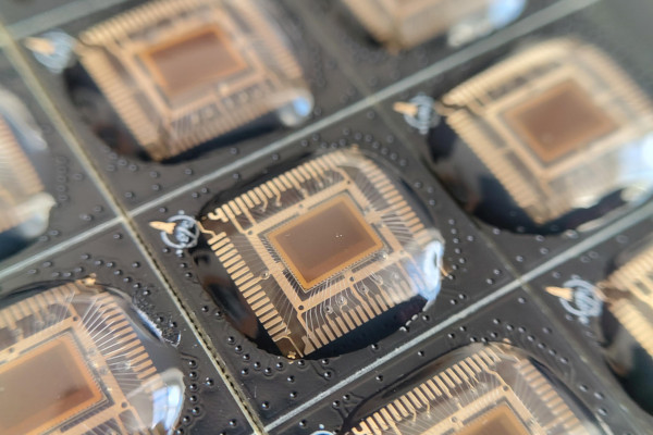
Tim opened the first wafer.space shuttle for submissions back in February, and chips from that run have begun landing. “wafer.space bare dies and CoB Chip-on-Board have arrived,” Leo Moser writes on Mastodon. “These are from my open-source FABulous FPGA, which was part of the first shuttle run. It’s a small FPGA with 480x LC, 6x MAC, 12x register files and 6x SRAM. The chip was implemented using the wafer.space LibreLane template and uses Yosys and nextpnr for the FPGA toolchain.”
“Fresh and custom silicon day,” adds Greg Davill in his own Mastodon post. “This is a multicore RISC-V SoC design based on the serv processor core. Based on GF180MCU PDK, and fabricated through wafer.space. I like that the COB is done with clear epoxy on these samples, rather than just a black blob.”
More information is available on the wafer.space website; those looking to be part of the second production run can purchase space on the upcoming GlobalFoundries GF180MCU shuttle on Crowd Supply, with pricing starting at $4,500 for 1,000 bare dies of a half-height or half-width design.
Dr. Semiconductor’s Home Fab Delivers DIY DRAM
Matthew Hartensveld, also known as YouTuber “Dr. Semiconductor," has demonstrated exactly what you can do if you build a class-100 cleanroom at the bottom of your garden - by making his own RAM chips.
“RAM prices have been insane,” Matthew says by way of introduction to his latest video. “Driven by the rise in AI, it is causing massive distruption to the GPU, cellphone, PC markets, and more. And a key reason it’s been so bad is that you have just three companies - Micron, Samsung, and SK Hynix - controlling the industry, where new supply is not something that can happen overnight. Building new fabs can take billions of dollars and years of work. So, rather than wait around I turned a shed in my backyard into a class-100 cleanroom and built my own semiconductor fabrication tools from scratch.”
Matthew’s work to build a do-it-yourself cleanroom was covered back in March, and progress has been rapid. From a bare shed to a working cleanroom with fabrication equipment in months, with the maker proving that everything’s functional by building working RAM chips at home.
“The transistor can very rapidly and quickly charge up our charge storage capacitor to 3V within a couple hundred nanoseconds, which is great,” Matthew says of the first parts to come out of the home fab. "And then it’ll hold that voltage on there but it’ll slightly bleed off over time, where we can only hold that charge on there for a little bit over two milliseconds before it’s completely done for. Commercial DRAM can hold its charge for greater than 64 milliseconds, so in this design it needs to be refreshed at a higher frequency.
“For the first time ever, RAM has been made at home. But while you can store data on it, you can’t run Doom on it quite yet: this is a just a few cells to prove it can work. The next step is to take these cells, stitch them together in order to make a much larger array - then we can hook it up to a PC.”
The full video walking through the entire design and manufacturing process is available on Matthew’s YouTube channel.
Greyhound, the Open RISC-V SoC and eFPGA, is Alive
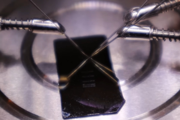
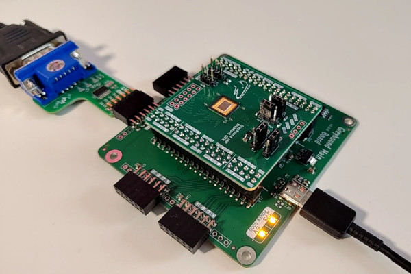
Leo Moser has announced a successful bring-up for the Greyhound RISC-V system-on-chip with embedded FPGA, following its fabrication in silicon on the IHP SG13G2 130nm process node.
“Greyhound is alive,” Leo wrote on Mastodon following the bring-up process for the custom chip. "I previously posted about soldering my custom chips onto breakout boards. Now, I can finally say that Greyhound is working. I’m incredibly happy that Greyhound is no longer just theoretical, but that it can run examples on its FPGA in the real world.
“This is the first version of Greyhound with an FPGA that has 784x LUT4s. Greyhound v2 with 1024x LUT4s is undergoing packaging and will be on its way soon. It’s a pin-compatible replacement, so bring-up should be straightforward too.”
Greyhound is a permissively-licensed RISC-V system-on-chip, built around the OpenHW CV32E40X core, with a FABulous embedded FPGA included in the design. “There is still much to be done,” Leo admits of the project and its ongoing testing. “While the FPGA is arguably Greyhound’s main feature, there’s also the RISC-V SoC and all the ways in which the two can communicate.”
More information is available in Leo’s Mastodon post and MakerTube video; Greyhound itself is published on GitHub under the permissive Apache 2.0 licence.
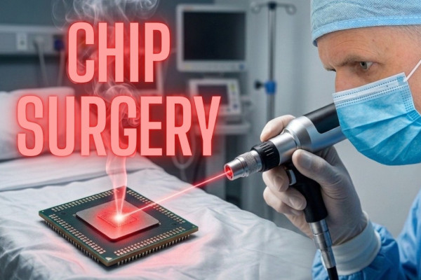
Matt Venn, Mikhail Svarichevsky Show Off Ion-Beam Chip Surgery
Tiny Tapeout founder Matt Venn has teamed up with Zeptobars’ Mikhail Svarichevsky to take full advantage of the open nature of chips produced under the multi-project shuttle effort - by modifying an already-produced chip with a focused ion beam.
“We cut a microscopic wire inside a chip with an ion beam, then brought it back to life with platinum gas,” Matt explains of the project, a video for which is due to air today. "It was quite tricky to find the design, as the top of the chip is full of regular repeating patterns, but because Tiny Tapeout chips are open source, we knew the exact co-ordinates of where to cut.
After focussing the ion beam we started blasting away the insulating layer covering the wires. One thing that surprised me was that we were able to see the hole being formed with the electron microscope, while the ion beam was cutting. After about 30 minutes the wires got thin enough to break and we saw the voltage drop to 0!
“The next step was to see if we could repair it,” Matt adds. “This technique involves injecting a platinum gas close to the working area, heating it up so it forms a thin conductive layer of platinum. It didn’t take long to see the voltage jump back to 3.3v.”
The pair’s video showcasing the project is due to air on YouTube at 1800 CEST/1600 UTC today, the 12th of May 2026; more information on Tiny Tapeout is available on the project website.

Researchers Highlight “Challenges and Opportunities” for Emulation-Based Verification
A team of researchers from the University of Florida’s Department of Electrical and Computer Engineering have released a paper detailing what they describe as “challenges and opportunities” for emulation-based security verification of systems-on-chips.
“Increasing system-on-chip (SoC) heterogeneity, deep hardware/software integration, and the proliferation of third-party intellectual property (IP) have brought security validation to the forefront of semiconductor design,” the researchers write. "While simulation and formal verification remain indispensable, they often struggle to expose vulnerabilities that emerge only under realistic execution conditions, long software-driven interactions, and adversarial stimuli.
"In this context, hardware emulation is emerging as an increasingly important pre-silicon verification technology because it enables higher-throughput execution of RTL designs under realistic hardware/software workloads while preserving sufficient fidelity for security-oriented analysis.
"This paper presents a comprehensive survey and perspective on emulation-based security verification and validation. We organise the landscape of prior work across assertion-based security checking, coverage-driven exploration, adversarial testing, information-flow tracking, fault injection, and side-channel-oriented evaluation. We provide a structured view of emulation-enabled security verification workflows, including instrumentation, stimulus generation, runtime monitoring, and evidence-driven analysis. We also examine practical challenges related to observability, scalability, property specification, and the definition of security-oriented coverage metrics for emulation-based verification.
“Finally,” the researchers’ abstract concludes, “we discuss emerging directions such as AI-assisted emulation, digital security twins, chiplet-scale security exploration, automated vulnerability assessment, and cloud-scale secure emulation. Overall, this paper positions emulation as a promising foundation for the next generation of pre-silicon hardware security assurance.”
A preprint of the full paper is available under open-access terms on arXiv.
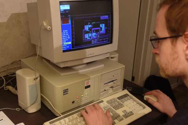
Video Shows How Far EDA Has Come Since 1995
The anonymous YouTuber and vintage computing enthusiast behind the Old Computers Sucked channel has highlighted just how things have changed in electronic design automation - by building a custom Motorola 68000-based computer from scratch using only the tools available in 1995.
“Why? Well, I just want to play more with hardware and explore things on a lower level than you’re normally able to do on a computer,” the presenter explains of the project’s inspiration. “I’ll be designing a PCB or PCBs that I’ll get etched and assembled. I’ll make a boot ROM for it, which will allow me to push new code to it over a serial port. And I want to be able to write a ‘hello, world’ program in C.”
While building a computer using off-the-shelf parts, like Motorola’s classic 68000 microprocessor, isn’t exactly the same as designing your own silicon, it’s not that different either - though the software you’d use today is a world away from what was available in 1995, when open-source tools were thin on the ground and your choice was either high-priced commercial offerings or typically closed-source shareware/freeware packages.
“I used a demo version of PADS, both the schematic program and the layout program,” the presenter explains. “It has some limitations on the complexity of the design you can make, but at least all the features are available. Make no mistake, though: PADS is the kind of program that requires you to read the manual. Without the manual, you’ll be completely lost.”
The full build process - from designing and producing the PCBs, programming generic array logic (GAL) chips, and developing software to run on the finished machine, all using only hardware and software available to the hobbyist in 1995 - is documented in the Old Computers Sucked YouTube video.
QEMU 11.0 Brings New RISC-V Extensions, Fixes
The latest release of the QEMU emulator, version 11.0, is out, and brings with it support for the RISC-V Zilsd, Zclsd, Zalasr, and Smpmpmt extensions - plus various compatibility and security fixes.
“We’d like to announce the availability of the QEMU 11.0.0 release. This release contains 2500+ commits from 237 authors,” the project maintainers write of the new release. “Thank you to everybody who contributed to this release, whether that was by writing code, reporting bugs, improving documentation, testing, or providing the project with CI resources. We couldn’t do these without you!”
The latest QEMU release brings with it support for four new extensions to the free and open RISC-V instruction set architecture: Zilsd and Zclsd, RV32-exclusive extensions to add register pair load and store instructions by reusing existing RV64-only instruction encodings; Zalasr, an atomic load-acquire store-release extension; and Smpmpmt, which provides a memory attribute control mechanism analogous to the RV64-only Rvpmt using PMP registers.
The full changelog is available on the QEMU wiki; releases are available on the project website, with full source code available on GitLab under the reciprocal GNU General Public Licence 2 or later.
Have feedback or news for inclusion in a future newsletter? Please send this to ecl@fossi-foundation.org.
Subscribe to get El Correo Libre direct to your inbox.